
The first installment of this Edge.Auto series explained why TIER IV is involved in the development of automotive cameras, featuring an overview of digital cameras and in-vehicle camera systems. This blog post covers image sensors – a core component of digital cameras – with a particular focus on the CMOS image sensors used in TIER IV’s C1 Camera and C2 Camera.
Charge-coupled device and CMOS
Almost all image sensors in devices manufactured today are CMOS image sensors, but until the late 2000s, the mainstream image sensor technology was a charge-coupled device (CCD). While both CCD and CMOS image sensors serve the same function of converting light into electrical signals, their structures and operating principles are significantly different.
CCD readout method
In the case of CCD, the charges generated by the photodiode are transferred to the readout circuit without amplification, and the signal is amplified in the final stage of the readout circuit.
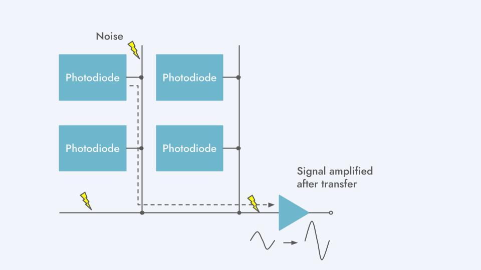 CCD signal transfer method
Charges read out from each pixel are transferred to the readout circuit through vertical and horizontal CCDs. Imagine a bucket brigade or conveyor belt, where the signal from each pixel is passed on to the neighboring pixel’s transfer section, one after another.
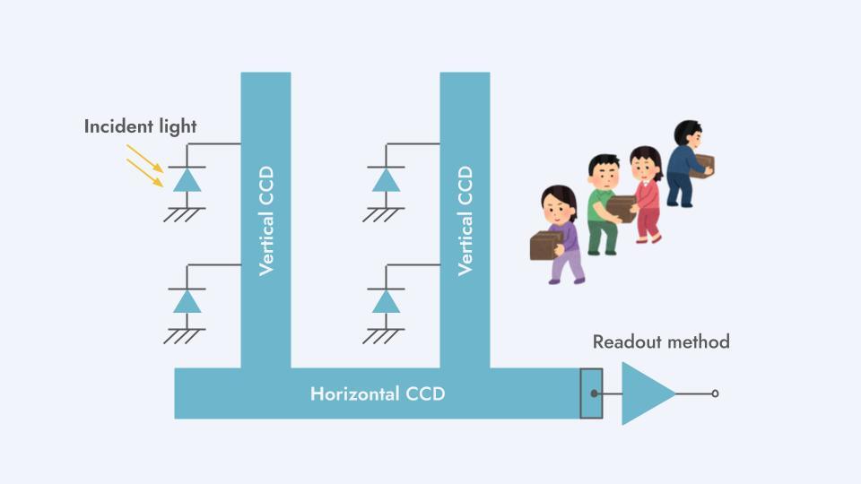 CCD structure
CMOS image sensor readout method
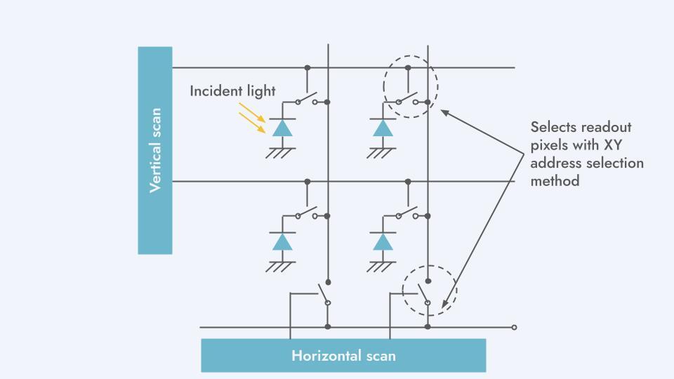
In the case of CMOS image sensors, the charges generated by each pixel are amplified by an amplifier circuit in each pixel. The readout is then performed by selecting each pixel using an XY address selection method.
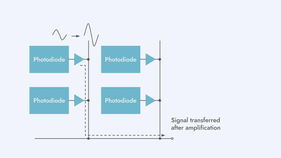 CMOS signal transfer method
The main differences in the operating principles of CCD and CMOS image sensors are as follows:
- CCD image sensors transfer signals and then amplify them. CMOS image sensors amplify signals and then transfer them.
- CCD image sensors use a bucket relay method for signal transfer, while CMOS image sensors use an XY address selection method.
CMOS structure
CMOS image sensors, which amplify the signal before transfer, are more resistant to noise on the signal transmission path. Another important point is that the XY address selection method offers greater flexibility in readout, allowing for forward scanning, reverse scanning, and skipping.
CMOS image sensor takeover
Transition from CCD
As mentioned earlier, in the evolution of image sensors, CCD initially led in practical applications but has since been replaced by CMOS image sensors. This shift occurred because CMOS image sensors could achieve the high image quality (high sensitivity, low dark current, etc.) previously realized by CCDs and there was increasing demand to integrate various functions into image sensors.
CMOS image sensors are manufactured using the complementary metal-oxide silicon process, similar to logic and analog semiconductors such as CPUs and GPUs. Therefore, in addition to the function of converting light into electrical signals, the same chip can include signal processing circuits, output circuits and analog-to-digital converters that convert electrical signals into digital values. This capability, known as system-on-chip integration, is one of the main advantages of CMOS image sensors.
For applications like digital video at full HD resolution or higher, high-speed signal readout is required. By integrating high-speed A/D converters in parallel with the pixel array, CMOS image sensors allow for rapid conversion of signals from photodiodes to digital, and efficient noise reduction, even at high readout speeds. These advantages have driven the transition from CCD to CMOS image sensors.
The ability of CMOS image sensors to operate at low voltage and low power consumption has also made it more suitable for devices like battery-powered mobile phones and smartphones, another factor that has fueled the transition.
Emergence of back-illuminated CMOS image sensors
An early drawback of CMOS image sensors was their lower sensitivity and angular response (sensitivity to light entering at an angle, crucial when using lenses with small F values). This was due to the multiple layers of wiring above the photodiodes in the sensor structure, causing light to be obstructed by these layers as it passed through. The solution to this problem came with the introduction of back-illuminated sensors.
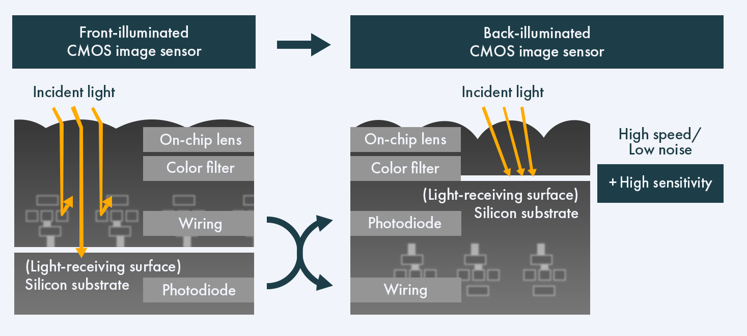
Source: Sony Semiconductor Solutions
In back-illuminated CMOS image sensors, the connection between the photodiode and wiring layers is inverted, with light entering the photodiode directly from the opposite side of the wiring layer. This increases the amount of light that can be captured by the photodiode. This configuration also prevents light from being obstructed by the wiring layers, enabling the sensor to capture light at larger incident angles and improving incident-angle characteristics.
Transition to stacked CMOS image sensors
In back-illuminated CMOS image sensors, the sensor is formed on a silicon wafer, thinly shaved and bonded to another silicon wafer called a support substrate. In stacked CMOS image sensors, the circuit is formed on the support substrate, separating the pixels from the circuit.
A stacked structure makes it possible to place the A/D converter and readout circuits, which were previously located around the pixel, on a separate chip (logic wafer), thereby reducing the chip’s footprint. Additionally, manufacturing the pixel wafer and logic wafer using separate processes allows for optimizing the manufacturing process for each according to their specific requirements and characteristics.
Currently, most high-performance CMOS image sensors are stacked, including the ones in TIER IV’s C1 Camera (ISX021) and C2 Camera (IMX490).
Structure of stacked image sensors
Stacked architectures comprise the following layers.
Microlens array
Above each pixel's photodiode, small lenses called microlenses are arranged in a regular pattern. Microlenses focus the incoming light through the lens onto each photodiode.
Color filter array
The photodiode itself cannot detect colors, but by placing color filters above it, specific colors can be selectively transmitted. This allows each photodiode to capture color information.
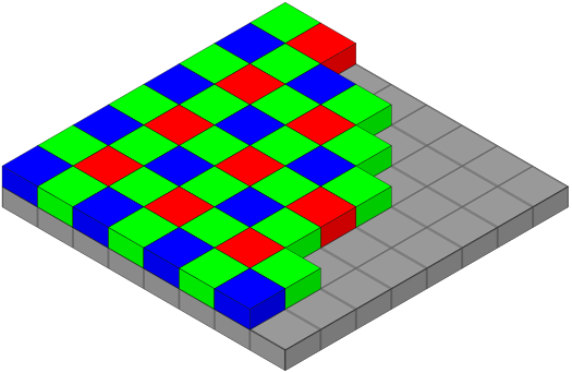
Bayer color filter pattern/Cburnett, CC BY-SA 3.0, via Wikimedia Commons
The arrangement of color filters commonly follows the Bayer pattern, which consists of a 2:1:1 ratio of Green/Red/Blue filters.
To enhance sensitivity in low-light conditions or improve color separation for specific wavelengths, manufacturers may use white (clear) filters, cyan, or yellow filters. This is an area where manufacturers of image sensors and image signal processors innovate to optimize their designs.
Photodiode
In photoelectric conversion, incident light is converted into electrical charge. Key performance metrics include the efficiency of converting incoming light into charge and the ability to suppress noise (known as dark current) when there is little or no incoming light.
Pixel transistors
The charge generated by the photodiode is amplified and converted into voltage or current. Typically, a single pixel includes the following:
- Reset transistor
- Transfer transistor
- Amp transistor
- Select transistor
To reduce pixel size, it's common for pixels to share transistors. Each pixel consists of a photodiode combined with pixel transistors. The size of pixels has been decreasing, with recent developments achieving pixel pitches below 1.0 µm, reaching as low as about 0.56 µm.
Bonding layer
The pixel chip with photodiodes and the logic chip with circuits are laminated to each other using a method called through-silicon via or copper-to-copper connection.
Application-specific integrated circuit (ASIC)
The logic wafer contains circuits that perform A/D conversion and subsequent signal processing beyond A/D conversion.
This blog post covered the differences between CCD and CMOS image sensors, the evolution of CMOS image sensors, and an overview of the structure of stacked sensors. The next installment will feature an overview of image sensor operation, covering global and rolling shutters. Stay tuned for future updates!
Yuichi Motohashi | Edge.Auto Team
Specializing in automotive CMOS image sensors and camera systems, Yuichi has been in charge of Edge.Auto cameras and development kits since 2023. Before joining TIER IV, he was involved in planning, developing, and commercialization of CMOS image sensors for automotive use, working with OEMs and Tier 1 suppliers in Europe and the United States.
TIER IV's automotive cameras, equipped with the stacked CMOS image sensor technology covered in this post, offer top-tier performance and reliability. With a high dynamic range of 120 dB, the C1 Camera (2.5 MP) and C2 Camera (5.4 MP) capture clear images in both bright and dark environments. Trusted by over 100 companies worldwide, these cameras are now available via the TIER IV store on Amazon.
TIER IV is always on the lookout for passionate individuals to join our journey. If you share our vision of making autonomous driving accessible to all, get in touch.
Visit our careers page to view all job openings.
If you’re uncertain about which roles align best with your experience, or if the current job openings don’t quite match your preferences, register your interest here. We’ll get in touch if a role that matches your experience becomes available, and schedule an informal interview.
Inquiries
- Media: pr@tier4.jp
- Business: sales@tier4.jp
Social Media
X (Japan/Global) | LinkedIn | Facebook | Instagram | YouTube
More